Description
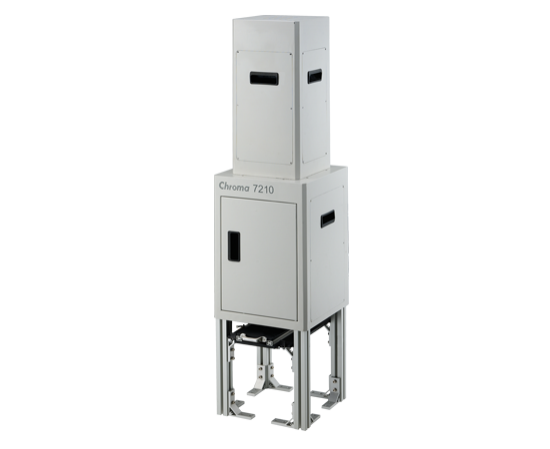
The Chroma 7210 has built two functions which are color sorting and printing inspection in one structure. With the compact “2 in 1” design, it not only optimizes the floor space but also maximizes the performance. As the “metallization” technology goes further in PV industry, the finger width has become narrower. Experts believe that practical finger width through “screen printing” technology would be narrower than 40μm in the near future, and Chroma’s 7210 is able to provide 33μm/pixel* solution for Photovoltaic technology innovators.
The Chroma c-Si cell coloring theory was designed to provide high repetitive color classification for c-Si PV cells. The CIE 1931 Lab color space and up to 60×60 grids for entire cell surface allow Chroma to provide numeric color severities down to 3600 blocks throughout the cell under test. Using the color information of each block and the customized algorithm, the user may determine the represented color for non-uniform color cells such as poly-crystalline cells or the cells have uneven anti-reflection coating thickness.
The defects caused by front-side (sunny side) printing process of c-Si PV cells may impact the performance, reliability or appearance. Therefore, a reliable and repetitive inspection of defects such as losing Ag paste on busbars, gridline interruptions, printing shift or rotation, water mark etc., has to be performed to ensure the quality before shipment. The Chroma 7210 solar cell quality classifier has equipped with a high resolution camera and superior software algorithm to recognize the unwanted defects on the front-side of c-Si PV cells.
The Chroma 7210 can be used right after the front-side process to retire cells with major defects. This allows best use of the capacity for the processes like I-V testing and sorting which are known as the bottlenecks of c-Si cell line.
The 7210 can be integrated into in-line or off-line sorter for final inspection prior to shipping.
Chroma 7210 can detected the Solar cell front side or back side surface defect and color classification.
The application of backside inspection, it is providing screen printing defect detection and color classification function when production the Bifacial products. When production the PERC products, it also providing screen printing defect detection function and detect the defects that generated by laser process.
Related Products

Anti-reflection Coating Inspector Model 7214-D
- Anti-reflection Coating Inspector
- Defects and color variance detection
- Install right after the PECVD or before the metallization process

Solar Cell Backside Printing and Surface Inspector Model 7213-AD
- Solar Cell Backside Printing & Surface Inspector (Diffuser type)
- V-cut and flake inspection
- Install on the metallization process and sorting process
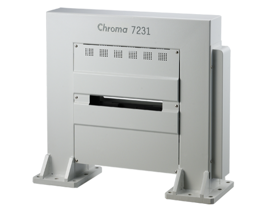
Solar Safer Sawmark Inspector Model 7231
- Solar wafer sawmark inspector
- EN-50513 2009 compliance
- High reliability

Solar Cell Frontside Printing and Surface Defect Inspector (High-Speed) Model 7212-HS
- Integrated with screen printing line and cell sorting lines from any manufacturers
- Flexible and intuitive SW user interface
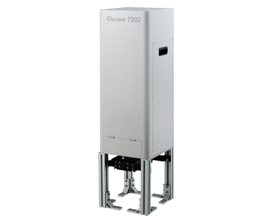
Solar Wafer Quality Inspector Model 7202
- Solar wafer quality inspector
- Accurate grain-size calculation
- Pinhole and chipping inspection
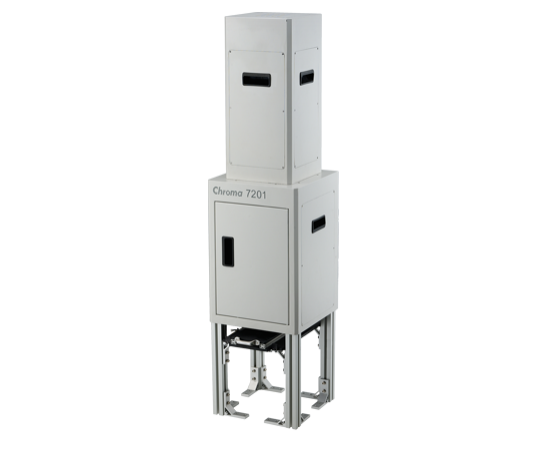
Solar Wafer Geometry and Surface Inspector Model 7201
- Solar wafer geometry and surface inspector
- RGB LED strobe lighting
- High speed inspection
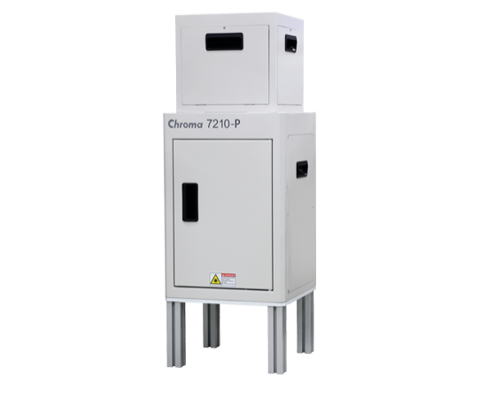
Printer Automatic Optical Inspector Model 7210-P
- Solar cell front-side printing defect inspector
- Detect the defects generated when fabricating PERC and Bifacial solar cells.
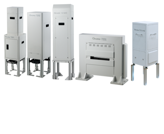
Automatic Optical Solar Cell/Wafer Inspection System Model 7200 Series
Chroma 7200 series are specially designed for detecting wide variety of defects observed for c-Si cells & wafers for all sizes and crystallizations.